Business
AP Systems, moving forward into the world with a passion for endless research and technological developments
Semiconductor
Sputter System
KORONA™ PVD600_ Advanced Package Process
- Semiconductor Advanced Package Sputter
- Following the high capacity, faster, and smaller trends of semiconductor devices, semiconductor Packaging technology has also been developed from the
previous Wire bonding to Flip Chip, and recently to FOWLP/FOPLP and 3D Packaging. - As the semiconductor Packaging technology is being developed, we at AP Systems, are providing client companies with Sputtering equipment for manufacturing
relevant metal films (CPB,UBM and RDL)
Technology
- Substrate Shift Detection & Align Technology when entering into each
chamber - ESC technology for low temperature (-20℃) to secure optimal process
(@ Preclearing & Process) - Multi Plate Heating System composition technology for Long Term Degas Time
(at least 30mins.) & High Temp. Uniformity
- Plasma Etching Chamber in the CCP form applied in Situ Pasting for the
Lower Particles - Magnetron Sputtering Source technology for High Film Quality and Film
Uniformity (Magnetron Scan & Tilt for FOPLP) - Verified Software Tool (Easy ClusterTM) operating technology applied to various semiconductor equipment
Features
PVD600: CPB & FOWLP
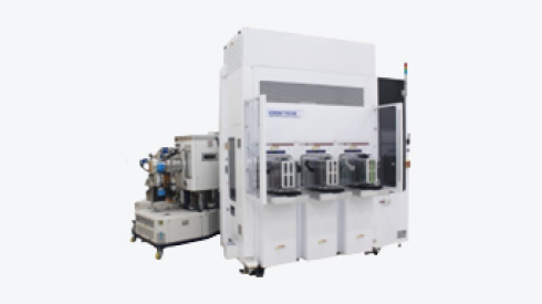
- Board Information: Diameter 300mm including EMC (Epoxy Molding Compound)
- EFEM, 2LoadLock, Octagonal Transfer Chamber, 2Multi_Degas Chamber,
2Pre-Cleaning Chamber (CCP) & 2Process Module
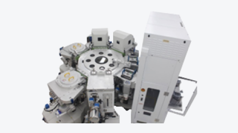
PVD600_R450: FOPLP
- Board Information: Rectangular (Approximately 400 x 500mm) type with PCB
- EFEM, 2LoadLock, Octagonal Transfer Chamber, 2Multi_Degas Chamber,
2Precleaning Chamber (CCP) & 2Process Module(Vertical Process)
Specification
| Temperature Uniformity> (@ Degas of 300℃) |
≤ 5% |
|---|---|
| Etch Uniformity (@ Precleaning) |
≤ 7% |
| Film Uniformity (@ Process) |
≤ 5% |
| Throughput (@ Ti : 1000Å, Cu : 3000Å) |
≥ 33 sheets/hr(@ Si기판), ≥ 24 sheets/hr(@ EMC & PCB 기판) |
Technology
- Wafer Shift Detection & Align Technology when entering into each chamber
- ESC technology for low temperature (-20℃) to secure optimal process
(@ Precleaning & Process) - Dual Heating System composition technology for Fast Temperature Rising
& High Temperature Uniformity
- Plasma Etching Chamber in the ICP form for Lower Damage & High Throughput
- Magnetron Sputtering Source technology for High Film Quality and Film
Uniformity (Magnetron Scan & Tilt for FOPLP) - Verified Software Tool (Easy ClusterTM) operating technology applied to various semiconductor equipment
Features
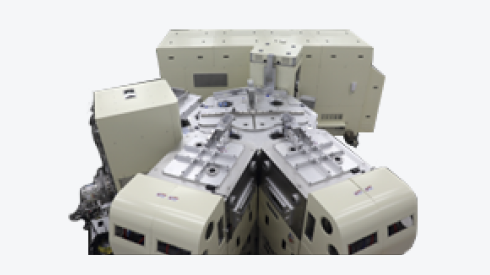
PVD600: Single Backbone
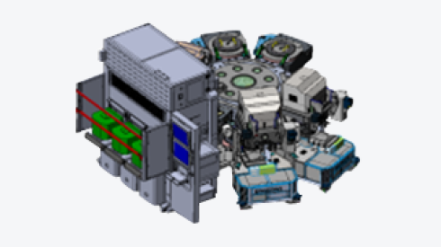
- EFEM, 2LoadLock, Octagonal Transfer Chamber, Single Degas Chamber, Pre-
Cleaning Chamber (ICP) & 2Process Module
PVD1000: Dual Backbone
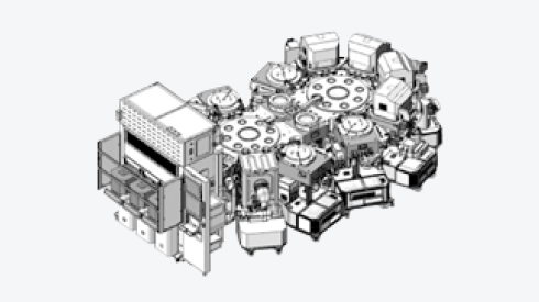
- EFEM, 2LoadLock, 2Octagonal Transfer Chamber, 2Single Degas Chamber,
2Precleaning Chamber (ICP) & 4Process Module
Specification
| Common | Temperature Uniformity(@ Degas of 300℃): ≤ 5% |
|---|---|
| Etch Uniformity(@ Pre-Cleaning) :≤ 5% | |
| Film Uniformity(@ Process) : ≤ 3% | |
| Throughput (@ Ti : 250Å, Al : 6000Å, TiN : 250Å) |
PVD600 : ≥ 39 sheets/hr |
| PVD1000 : ≥ 52 sheets/hr |
