Business
AP Systems, moving forward into the world with a passion for endless research and technological developments
Semiconductor
-
Semiconductor
- Rapid Thermal Process
- Sputter System
- Descum System
- Laser Dicing
- Laser De-bonder
- Wafer Dicing
- Laser Annealing
- Laser Ablation
-
Display
-
Front-End Process
- Excimer Laser Annealing
- Laser Lift-Off
- Glass Encapsulation
- ALD
- Film Laser Cutting
- PECVD
-
Back-End Process
- Module Lamination
- Module Dispenser
- Module OCR Inkjet
-
Front-End Process
-
EV Battery
- NG SORTER
- TRAY WASHER
- CELL TAPING
- CELL PACKING
-
Solar Cell
- LEI
- LDSE
- LCO
-
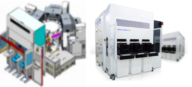 Rapid Thermal Process
Rapid Thermal Processing(RTP) equipment, which treats wafers with high temperature in a short time using tungsten halogen lamps, is applied to various processes such as implantation and diffusion.
-
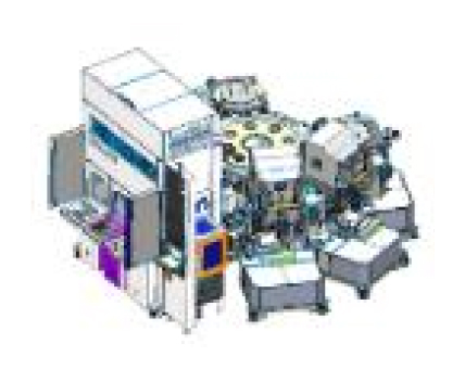 Sputter System
Following the high capacity, faster, and smaller trends of semiconductor devices, semiconductor Packaging technology has also been developed from the previous Wire bonding to Flip Chip, and recently to FOWLP/FOPLP and 3D Packaging. As the semiconductor Packaging technology is being developed, we at AP Systems, are providing client companies with Sputtering equipment for manufacturing relevant metal films (CPB,UBM and RDL).
-
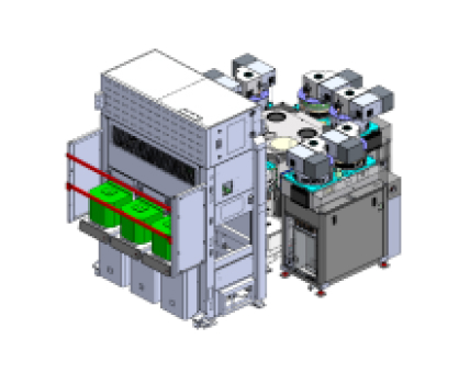 Descum System
It is a plasma treatment system that removes scums in the lateral walls of the pattern before electroplating, or performs surface modification to improve adhesive power, when forming Bump to be used in Flip Chip Bonding in the wafer.
-
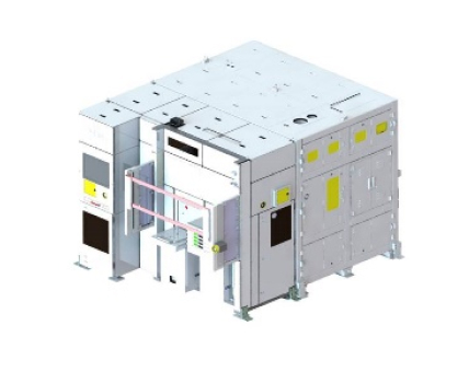 Laser Dicing
This equipment is used in semiconductor analysis processes to cut and separate semiconductor chips mounted on a wafer into individual cells using lasers and high-precision scanner optics.
-
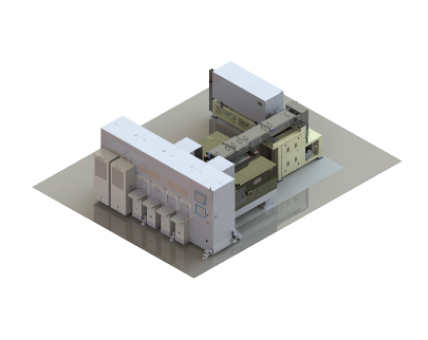 Laser De-bonder(KORONA TM LD)
The manufacturing process equipment used in semiconductor HBM, WLP, and PLP manufacturing processes utilizes laser technology, optical systems, and process modules to separate the device substrate from the carrier substrate.
-
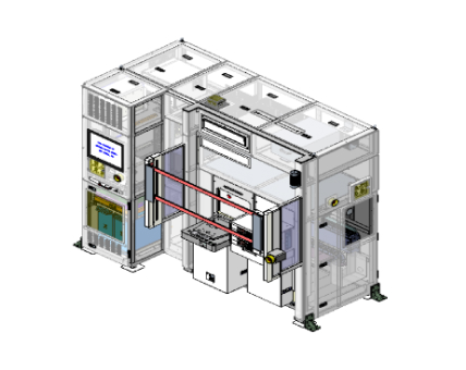 Wafer Dicing
This manufacturing process equipment cuts and separates semiconductor chips mounted on a wafer into individual cells.
-
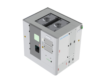 Laser Annealing
This process equipment selectively heat-treats the wafer surface according to the intended purpose using a triple-wavelength laser during the front-end semiconductor process. Purpose: Dopant Activation, Silicidation, etc.
-
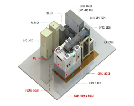 Laser Ablation
This process equipment is used in semiconductor packaging processes to selectively remove insulating materials.
